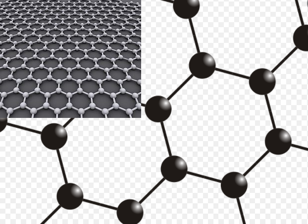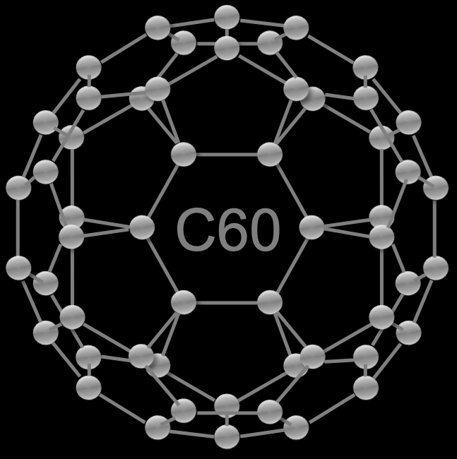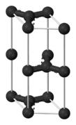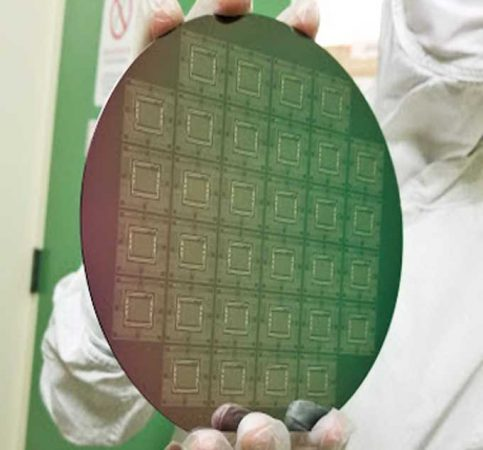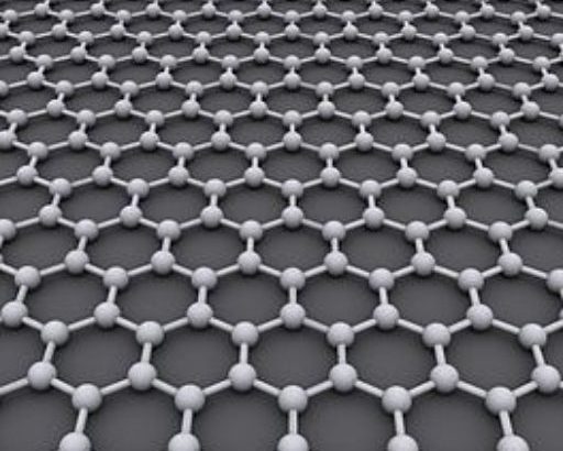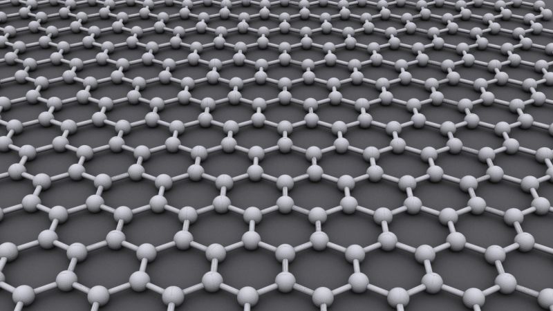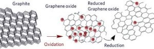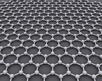
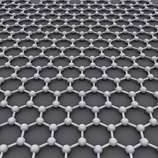
Graphene is a material that is extracted from graphite and is made up of pure carbon, one of the most important elements in nature and which we find in daily objects like the lead of a pencil.

Graphene stands out for being tough, flexible, light, and with a high resistance. It’s calculated that this material is 200 times more resistant than steel and five times lighter than aluminum.
With these properties, graphene has applications in the energy, construction, health, and electronics sectors. For instance, magnetic graphene could transform this electronics industry by making devices more comfortable and accessible for everyone.
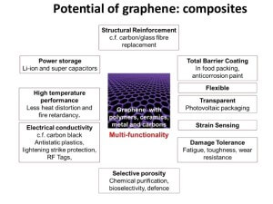
Graphene has a wide range of potential applications and uses due to its exceptional mechanical, electrical, and thermal properties. It is used in electronics, energy storage, sensors, coatings, composites, biomedical devices and many other. Its high surface area and biocompatibility make it an attractive material for drug delivery and tissue engineering applications. Graphene’s unique properties make it a promising material for many future technologies.
Energy Industry Uses & Applications of Graphene
1. Graphene in Solar Cells
The idea of developing lighter, flexible and transparent solar cells has been around for a while but finding the material which has all the properties and able to carry the current was the issue. Indium Tin Oxide has been used because it was transparent, however it was not flexible therefore the cell had to remain stiff.
In 2017, researchers from MIT have managed to apply and use graphene succesfully on a solar cell. When they compared the graphene solar cell with others made of Aluminum and Indium Tin Oxide, they saw that it was as good as the ITO cell, and a little worse than Al one in terms of current densities and power conversion efficiencies. However, it is expected for a transparent cell to perform lower than Aluminum-based, which is nontransparent.
Although electrical properties were not a breakthrough, a solar cell that can be installed on any kind of surface (cars, clothes, paper, and cell phones, etc.) which is flexible and transparent was developed. Moreover, other scientists are trying to find out if graphene solar cells can generate energy from raindrops, which theoretically looks possible.
2. Graphene in Batteries
Graphene enhanced Li-ion batteries show incredible characteristics such as longer lifespan, higher capacity, and faster charging time as well as flexibility and lightness, so that it could be used in wearable electronics.
3. Graphene in Nuclear Power Plants
Heavy water used in nuclear power plants to cool the reactors is both costly to produce and causes a million tons of CO2 emissions during production. Researchers from University of Manchester have discovered that there is a greener and low-cost method to produce heavy water: graphene membranes. Team leader Dr. Lozada-Hidalgo believes that this innovation is extremely important and its introduction to the nuclear industry will be soon even though this industry is usually skeptical about new technologies.
4. Graphene in Thermoelectric
Seebeck effect is defined as a thermoelectric effect occurring when heat is applied to one of the two dissimilar electric conductors (or semiconductors) to move the electrons from the hot part to the cooler part and produce electricity. However, the energy generated by this method is really small, usually quantified by microvolts. Still, it is believed that it can be used to benefit from the heat generated by the engines, which is practically wasted. Graphene can be used to increase the Seebeck effect created by Strontium Titanate, almost up to 5 times.
5. Graphene in Alcohol Distillation
Graphene’s physical properties is so interesting and unique that, it would let large water molecules to pass through but stop Helium molecules which could leak through glass. Andre Geim (one of the inventors of Graphene) and Rahul Nair from Manchester University have tried sealing a bottle of vodka with graphene membrane that they have developed, and discovered that graphene could distill ethanol effectively even at room temperature and without the vacuum needed for distillation methods. This area of utilization can be employed in alcoholic beverages, fuel, water purification and so on.
6. Graphene in Fuel Cells
Even hydrogen atoms, known as the smallest atom, cannot pass through Graphene. In another research, Sir Andre Geim and his team have tested if protons would be blocked by graphene or not. Suprisingly, protons could pass through graphene. This property would improve fuel cells performance by lowering the fuel crossover which is a major problem with fuel cells that decreases durability and efficiency.
Medicine Uses & Applications of Graphene
7. Graphene in Drug Delivery
Functionalized graphene can be used to carry chemotherapy drugs to tumors for cancer patients. Graphene based carriers targeted cancer cells better and reduced and decreased toxicity of the effected healthy cells. Drug delivery is not limited to cancer treatment, anti-inflammatory drugs have also been carried by graphene & chitosan combinations and yielded promising results.
8. Graphene in Cancer Treatment
Graphene can also detect cancer cells in the early stages of the disease. Moreover, it can stop them from growing any further in many types of cancer by intervening the correct formation of the tumor or causing autophagy which leads to the death of cancer cells.
9. Graphene in Gene Delivery
Gene delivery is a method used to cure some genetic diseases by bringing foreign DNA into cells. Graphene Oxide modified by Polyethyleneimine can be used for these purposes is expected to show low cytotoxicity, as it did in the drug delivery case.
10. Graphene in Photothermal Therapy
Photothermal therapy (PTT) is a approach used to eliminate abnormal cells in the targeted area of the body by irradiating a special agent which creates heat capable of destructing those cells. Graphene oxide increases effectiveness of PTT by a number of ways. First, it can be used to carry chemotherapeutic drugs to the tumor cells while they are being exposed to PTT simultaneously. Combining chemo and PTT like this is more effective than using one of these approaches alone. A nanocomposite of reduced graphene oxide (QD-CRGO) can be used during PTT for bioimaging of the cancer cells. Moreover, in their research, a group of scientists from Texas Tech and Texas A&M University have shown that using graphene oxide functionalized with biocompatible porphyrin as a platform for PTT for brain cancer have killed more cancer cells than PTT alone, while giving no harm to the healthy cells.
11. Graphene in Diabetes Monitoring
Scientists from the University of Bath have developed a blood glucose monitoring test which does not pierce the skin, unlike currently used finger prick tests. This patch, including a graphene sensor, is able to work on a small area containing at least one hair follicle. It detects the glucose by pulling it from the fluid present between the cells. This does not only end the painful methods of blood sugar monitoring, but is also expected to increase the accuracy of the results.
12. Graphene in Dialysis
Graphene membranes are not only useful for the energy, nuclear and food industries. A group of researchers from MIT showed that graphene can be used to filter the blood from wastes, drugs and chemicals as well. Graphene’s superiority in this case is that it is 20 times thinner than traditional membranes which leads to significant decrease in the time spent in the dialysis for the patients.
13. Graphene in Bone and Teeth Implantation
Hydroxyapatite, a form of calcium apatite, is a material used as a synthetic bone substitute for regenerated bone and dental tissues. Graphene, combined with Hydroxyapatite and Chitosan, have shown increase in the strength, corrosion resistance, flexibility and mechanical & osteogenic properties of the substitute when compared to HAp alone.
14. Graphene in Tissue Engineering and Cell Therapy
Bones are not the only tissue graphene can cure. Certain forms of graphene were shown to be compatible with human osteoblasts and human mesenchymal cells, showing similar properties with the cells’ physiological microenvironment. Cells grown with this method demonstrated better growth, proliferation, and differentiation while being ineffective on the cells’ viability. Stem cells are especially important in tissue reengineering to improve the lives of people with neuronal disorders or neurodegenerative diseases.
15. Graphene UV Sensors
UV sensors are used for detecting dangerous levels of ultra-violet radiation which can lead to skin problems or even cancer. However, it is not the only use of UV sensors, they are used in the military, optical communication, and environmental monitoring as well. On its own, graphene may not present a high photoresponsivity but when it is combined with other materials, they create flexible, transparent, environmentally-friendly and low-cost UV sensors which will lead to technologies such as wearable electronics in the close future.
16. Graphene for the Brain
Mysteries about the brain haven’t been revealed completely yet. A graphene-based technology may allow scientists to uncover many of the unknowns by recording brains electrical activity. This new device is able to hear the frequencies below older technologies’ limits, and it doesn’t interfere with the functioning of the brain. Besides research on how the brain works, the technology can help the scientists to understand the reasons behind epilepsy seizures and develop treatments for the patients. Moreover, discovering more about the brain could lead to developing new Brain-Computer interfaces which are used in many areas including control of prosthetic limbs.
17. Graphene in HIV Diagnosis
Despite all the improvements, there are many drawbacks on current HIV diagnosis methods. They can either detect the antibodies in the body nearly a month later the patient was infected, or they can detect the virus itself however these methods take some time to process themselves and more expensive when compared to the antibody method. A biosensor made of silicon or graphene, containing Gold Nanoparticles was developed by Spanish National Research Council, which targets p24, an antigen found on HIV. The new method can detect the virus only a week after being infected and at levels 100,000 times lower than what the current tests can notice. Moreover, results of the test are ready within 5 hours of being tested.
18. Graphene Biosensors
One of the advantages of graphene is its ability to detect minimal amounts of substances. Even a single molecule in a large volume can be detected with it. Biosensors made of graphene, graphene oxide or reduced graphene oxide show ultrasensitive properties when detecting DNA, ATP, dopamine, oligonucleotides, thrombin, and different atoms. There are several medical companies that already sell medical sensors made with graphene.
19. Graphene Bactericide
Graphene is a magnificent bactericidal material as it avoids the generation of microorganisms, such as bacteria, viruses, and fungi, by damaging their cell membranes between its outer layers. When compared to different derivatives of Graphene, Graphene Oxide and reduced Graphene Oxide shows the best antibacterial effects. GO can also be used as a compound with silver nanoparticles to increase antibacterial properties even further.
20. Graphene in Birth Control
Graphene has all the properties that is desired in a condom: it is flexible, extra strong and extremely thin. Researchers from Manchester University have worked on developing a “supercondom” made of graphene and latex combined. The research has received many funding, including one from Bill and Melinda Gates Foundation.
21. Graphene in Deaf-Mute Communication
A group of Chinese scientists have developed a wearable, bio-integrated device that can translate sign language into text and spoken language. The device uses graphene’s incredible conductivity and flexibility properties.
22. Graphene in Body Scans
Unlike X-rays, T-waves which can be used for body scanning are harmless to human body. However, there is a catch. T-waves, or THZ radiation, is hard to both detect and generate. The good news is, with the help of some modifications and other materials, CVD graphene can detect THZ radiation successfully. This will not only lead to safer body scans, but also incredibly faster internet in the future.
Electronics Uses & Applications of Graphene
23. Graphene in Generating Light
Researchers at MIT have discovered that when light hits the surface of graphene, it’s slowed down and the photons started moving in a speed very close to the speed of electrons which increases when moving on graphene. This coincidence makes it possible to break the light barrier for electrons and creates light. The advantage of this method over the conventional ways of generating light such as fluorescent or LEDs is that it’s expected to be more efficient, faster, compact and controllable, and it looks like generating light from graphene will be a key milestone in developing even smaller, faster and more efficient computer chips.
24. Graphene Transistors
The new supertransistors, which replace silicon with graphene, can increase the speed of computers up to one thousand times when compared to current technology. Increasing speed of computers is a crucial step for many technologies to be able to improve, including but not limited to blockchain, simulations of the outer space, robots, and stock markets.
25. Graphene in Waterproof Electronics
One of the main problems of electronic devices which people are afraid of is being dropped to water. Instead of covering the device with tight-fitted screws, graphene proposes a great solution for this problem. Engineers from Iowa State University print the circuits of the device with graphene flakes because graphene is transparent, strong and conducts electricity. Graphene flakes are arranged in a specific order and non-conductive binders are used to combine them which improved the conductivity. As in the most application areas, graphene again puts a great solution to this problem.
26. Graphene in Wearable Electronics
Researchers are looking for new ways to power wearable devices. One of the outstanding ways is flexible batteries printed on a fabric with graphene. This enables people to wear their batteries and power their smartphones or other devices, literally. If this can be achieved, it will be an environmentally friendly and smart e-textile that can store energy. Carrying heavy power-banks or chargers will be history by the invention of this amazing idea.
27. Graphene for Touchscreens
Indium tin oxide (ITO) is the commercial product used as transparent conductor of the smartphones, tablets, and computers. Researchers from the Rice University have developed a graphene-based thin film to be used in touchscreens. It is found that graphene-based thin film beats ITO and any other materials in terms of performance because it has lower resistance and higher transparency. Thus, Graphene is the new candidate material for the replacement of ITO.
28. Graphene in Flexible Screens
The world of technology would be one of the great beneficiaries of the standardization of graphene as a material to incorporate in products such as smartphones or tablets. It would be the definitive step to advance in the world of smartphones.
Recently, a Chinese company has produced a bendable smartphone with a graphene touch screen. Since one layer of graphene is strong, light, transparent and very conductive, it meets all the requirements for the production of smartphones. The smartphone of the Chinese company has the ability to wrap a twist completely, and it weighs only 200 grams which propose a perfect convenience for usage. However, production of graphene is expensive at an industrial scale relative to other materials used in smartphones. Researchers are looking for ways to produce graphene at lower costs. When this problem and some others are solved, old phones seem to be replaced by these flexible smartphones in the future. Nanografi’s Europe Horizon 2020 winner project: Green Graphene, producing top-tier Graphene with environmentally friendly methods and lowest costs.
29. Graphene in Hard Drives and Memories
Usually, graphene is not considered magnetic, at least not in a controllable or useful way. In 2015, researchers from U.S. Naval Research Laboratory have found a way to turn graphene into a reliable and controllable electromagnetic material. If this innovation is used in hard drives, it is expected to have a capacity almost a million times greater than what we use today.
30. Graphene in Elastic Robots
A team of researchers has developed a gel that is sensitive to near infrared light so that it could be used in numerous applications when creating flexible or elastic robotic parts. The snake-like robots created with this method are able to change its form without any forces from the outside. Their future applications can vary from search-and-rescue to medical operations.
31. Graphene as a Superconductor
Scientists have discovered that graphene can also be used as a superconductive material. Two layers of Graphene can conduct the electron without any resistance. This can be accomplished by twisting these two layers of graphene at a ‘magic angle’ which is 1.1°. Most of the superconductive materials show their properties at temperatures close to absolute zero. Even High temperature superconductive materials relative to usual ones can work at around -140°C. In other words, these superconductive materials require a huge energy for cooling. If graphene can be used as a superconductive material at temperatures close to room temperature, there will be a huge revolution for many application areas.
32. Graphene in Optoelectronics
Researchers are working on a new material for the optical communications since energy and power requirement increase as the time passes. A research conducted by the collaboration of different universities has shown that integrating graphene with silicon can beat current silicon photonic technology. How can it beat the current state of art? Because devices made by graphene are cheaper, simpler and work at high-scale wavelengths. Apparently, graphene will present a low-energy optical telecommunication and many other convenient optical systems.
33. Graphene in Optical Sensors
Graphene has a lot of breakthroughs in industry and science owing to its super properties. Researchers tried to shrink the light to make optical sensors smaller. Recently, the Institute of Photonic Sciences (ICFO) in Barcelona, with the collaboration of Graphene Flagship team, conducted a study which explains the reduction of light down to just a single atom thick which is thought to be impossible by many researchers. This discovery will lead to a huge step in ultra-small optical sensors and switches.
34. Graphene Security Sensors
One of the first practical and real applications of graphene was security labels. Instead of the bulky sensors that many stores use, the sensors made with graphene are smaller, more aesthetic, able to bend without creating a damage on the circuit, and cost only a couple cents per tag.
Food Industry Uses & Applications of Graphene
35. Graphene in Food Packaging
Graphene can also be used as a coating material because it prevents the transfer of water and oxygen. Graphene membranes can be used in food or pharmaceutical packaging by keeping food and medicines fresh for longer time. It may seem a simple application, but it can dramatically reduce the amount of food waste people throw away every day.
36. Graphene in Water Purification
Normally, water purification is not a simple process and feasibility of the process depends on how heavily the water is contaminated. An Australian scientist has found a low-cost technique to purify water at one step. Soybean-based graphene, which is also called ‘GrapHair’, is used as a filter. This filter can make the dirtiest water drinkable. it is more efficient, cheaper and environmentally friendly compared to other methods.
37. Graphene in Desalination
Approximately, 97.5% of the total water present on the planet is salty. It does not matter how many wells we excavate, only 2.5% of the total is fresh water. The filters based on meshes that use graphene have yielded amazing results. The University of Manchester employed graphene to make filtering sieve that has higher density and permit the water particles to pass but prevents the salts.
38. Graphene in Crop Protection
Graphene is a great material for sensors. Micro-sized sensors can be produced thanks to graphene’s unique structure. It can detect whether a molecule is dangerous or not for the environment. These sensors can be used in food industry, especially in crop protection. Farmers can track and detect dangerous and harmful gasses to crop and they can determine the ideal areas for the growth of the crop depending on the atmospheric conditions, and even the moisture level and “thirst” of the plants with the help of graphene sensors.
39. Graphene for Food Security
Studies done by US Rice University have shown that laser-induced graphene can be applied to various substances such as wood, bread, coconut, etc. It may seem like a substance with a pattern on it printed with ink, but it is not. The laser carburizes the material and carburized material is converted into graphene. Any pattern that is desired can be achieved by this technique. Issues that are related to food security can be overcame by this technique.
Sports Equipment and Technology Uses & Applications of Graphene
40. Graphene in Shoes
Graphene sneakers? Yes, although in this case it is not used purely, other composite materials take advantage of it. In fact, it is claimed that a sole made of pure graphene could last hundreds of years. University of Manchester and sports brand Inov-8 developed a shoe using graphene which increases the outsoles’ strength and flexibility properties by 50%. These shoes are more durable and absorbs the impacts which could damage the bones and joints.
41. Graphene in Helmets
An ideal helmet would be strong, resistant to impact, durable, comfortable, and light. Graphene is incredibly strong, light, and flexible. It’s even used in bulletproof vests, so it can definitely resist impacts. With these properties, graphene is commercially used in motorbike helmets.
42. Graphene in Tires
Graphene is also used to make smarter tires and sports bike components. Adding graphene to bike’s tires apparently increases the puncture resistance and velocity, decreases rolling resistance and makes them way lighter, stronger, faster, and more resilient.
43. Graphene Clothes
The use of graphene fibers in fabrics offers antibacterial, and anti-static clothes which can preserve the heat and block UV. These fabrics can be used to create outdoor sportswear, pajamas for children that repel soil bacteria, or even household furniture to prevent the development of bacteria on its surface.
44.Graphene Rackets
Graphene can improve the energy distribution and weight of the racket while increasing the service speed and stability. Tennis equipment manufacturer Head have already developed a series of commercially available racket enhanced with graphene, named “Graphene 360” which is already used by tennis stars like Novak Djokovic and Sascha Zverev.
45. Graphene Electronic Tattoos and Fitness Tracking
Graphene Electronic Tattoo (GET) is developed by scientists at the University of Texas. First, they are more resistant to moisture, have a greater elasticity – with the ability to grow or shrink up to 40%, have a total thickness of 463 ± 30 nm, and have optical transparency of approximately 85%. They are like a second skin. These tattoos can be used to track heart rate, temperature, hydration levels, oxygen saturation and even the level of exposure to UV. Their application areas can vary from fitness tracking to medicine.
Other Uses & Applications of Graphene
46. Graphene and Silk
Researchers in China have conducted a research to enhance the properties of silk which has already great characteristics. Silkworms eat white mulberry leaves. Researchers sprayed a solution having 0.2 percent graphene on the leaves and let the silkworms eat that leaves. Findings were promising because commercial silkworms fed by graphene sprayed leaves give ten times more than what a usual silkworm can. While it is uncertain how much of the graphene is digested by silkworms, this study will have a positive effect on smart clothing which is a hot topic of the recent years.
47. Graphene in Cement
Potential application areas of graphene expand as the time passes. One of the important potential usages of graphene is construction industry because graphene is strong and light at the same the which is perfect for construction. It can be used instead of steel, but strength and weight are not the only parameters. Graphene’s the main problem is that crack propagates very fast in graphene which can cause catastrophic failures. Researchers are trying to find ways for using graphene in construction. A group of researchers from University of Exeter used graphene in cement as a reinforcement material and tested. As a result, 2.5 times stronger and 4 times less water permeable concrete was obtained which proves that graphene can be a great reinforcement material in construction.
48. Graphene in Insulation
Graphene can be used as a superconductor or insulator material when two sheets of graphene are arranged at a magic angle. Most of the metal parts of the cars, ships or planes suffer from rusting. When graphene is combined with paint, it can be a great insulation material for creating rust-free surfaces. Another application can be coating of bricks and stones. In this way, water-proof houses can be constructed.
49. Graphene in Speakers and Headphones
A speaker converts electricity into sound by vibrating a membrane in the air. Graphene is used to make lightweight and great rigidity membranes. Moreover, headphones use a small diaphragm reinforced with graphene. GrapheneQ, a headphone developed by the company ORA Sound is lighter and smaller, and at the same time it can reach louder and higher quality sounds with less energy.
50.Graphene in Photography
Due to its exceptional properties and high sensitivity to ultraviolet, visible and infrared lights, graphene seems to be one of the ideal materials to push digital photography and any discipline where optical modulators and photoreceptors are involved. Cameras’ sensors enhanced with graphene and quantum dot can be smaller and lighter while achieving greater resolution levels than any small sensor could up until now.
51. Graphene in Automotive
The extraordinary strength and hardness of graphene, coupled with its flexibility, is perfect to start creating cars that are immune to shocks. Moreover, accident-proof vehicles could also be created. This would result in a direct decline in road mortality. Graphene cars, which we may see in the showrooms within a decade, are also expected to be cheaper and lighter.
52. Graphene in Airplanes
Scientists from UK have designed an airplane that includes graphene in the carbon-fiber coating of the aircraft’s wings. The model plane, Prospero, was lighter since it was enough to cover the wings with only one layer of the improved composite. It consumes less fuel, resists impact better, and has lower environmental costs as well.
53. Graphene Paints
Every painter knows it very well: humidity is the number one enemy of painting. Graphenstone is a company that makes graphene painting solutions. The result? The light bounces better, protects barrels and basements, absorbs 120 grams of CO2 per square meter and is able to withstand the corrosion derived from contact with metals.
54. Graphene in Ballistics
Kevlar is used in the manufacturing of bulletproof vests, helmets and protective clothing and even weapons. But graphene has much greater malleability and is medically safer in case of accident and contact with the bloodstream. Moreover, Kevlar and graphene composites are lighter to wear, and increases heat absorption for the protection of the fibers, when compared to Kevlar on its own.
55. Graphene in Military Protective Equipment
One of the future uses that have been raised for graphene is destined for the arms industry. In particular, its usefulness would be aimed at shielding and protection. It could be used in making helmets, bulletproof vests, and many more accessories. It could, in fact, graphene will be a determining material for the future of police forces and armies.
56. Graphene in Thermal and Infrared Vision
A great advance that we could see is the development of graphene lenses that allows thermal and infrared vision. The graphene allows manufacturing such ultrathin devices with a built-in camera that gives the user an infrared and thermal vision. Something that until now we have only seen in science fiction movies.
57. Graphene in Machinery Lubricants
Industrial machines mostly suffer from friction because friction affects the durability, strength, efficiency and working life of the machines negatively. To minimize these effects, solid or liquid lubricants are used. Recently, graphene, which has countless potential application areas, has started to shine out on this subject. Why graphene? Because it offers perfect friction and wear properties compared to conventional materials. It can also serve as solid or liquid lubricant. In addition, having a great chemical inertness, smooth and densely packed surface makes graphene a great lubricant material.
58. Graphene in Corrosion Protection for Glass
One of the application areas of graphene is that it can be used as a coating material for glass. Although glass is a high resistant material to corrosion, it can corrode under some conditions such as high humidity or extreme pH values. Also, durability of the glass can be vital in some areas such as pharmaceutical or optical industries. It prevents any type of failure such as corrosion, oxidation, electromagnetic radiation. Graphene with high transparency and high chemical inertness can be a promising material for the protection of glass.
59. Graphene in Radiation Shielding
Scientists have been trying to keep the radiation at minimum since it is very dangerous for human health. For this purpose, a variety of materials can be used as a shielding material to radiation but there are many parameters that affects the efficiency of shielding. Graphene is known as a weak radiation absorber, but scientists have found that it can be a great shielding material when it is used in multi-layered form which are graphene slabs. Graphene is an outstanding material for this purpose thanks to its low manufacturing cost, light weight and high efficiency compared to any other shielding materials.
60. Graphene for Anti-corrosion Oil and Gas Pipes
Underwater pipes used to carry oil or gas is subject to corrosion over time, as CO2 and water is able to get through the outer layers sometimes. Repairing them is costly, and if they break due to the corrosion, they would release the content which may be toxic to aquatic life. Researchers from the University of Manchester and the technology firm TWI have developed a coating with graphene nanoplatelets and tested it under the temperature and pressure conditions the pipes would face under the sea. The result was that, CO2 permeability was decreased by 90%, and lowered the permeability of other corroding agents as well.
Could not find an application of graphene that you know of? Or saw one which is outdated and no longer valid? Graphene is an emerging material with.
Conclusion
In conclusion, graphene is an extraordinary material that has sparked a global rush in industry. It’s composed of pure carbon and possesses remarkable properties, including its strength, lightweight, and conductivity.Graphene has endless potential applications in electronics, energy storage, sensors, coatings, composites, and biomedical devices. Its high surface area and biocompatibility make it an attractive material for drug delivery and tissue engineering applications. Nanografi offers high-quality graphene and nanotechnology solutions to enhance a range of projects, productions, and technologies. Overall, graphene’s unique properties offer an exciting new frontier in technology and have the potential to revolutionize many industries in the future.