Pelletized Activated Carbon and Its Usages

Pellet activated carbon produced from coal, wood and coconut shell, either by high temperature steam activation or chemical activation under stringent quality control. With low ash content, large surface area, high mechanical hardness, high pore volume and chemical stability.

By varying manufacturing conditions, internal pore structures are created that impart unique adsorption properties specific to each product type. The choice of product for a specific application will vary due to differing impurities and process conditions.

Pelletized activated carbon is created by extruding activated carbon into cylindrical shaped pellets with diameters ranging from 0.8 to 5 mm. Their high activity and surface area make it ideal for many vapor phase applications. The uniformity of its shape makes it particularly useful in applications where low-pressure drop is a consideration.

Pelletized activated carbon provides lower pressure drop than granular activated carbon in fixed-bed purification of gases and vapors. The adsorptive capacity of pelletized carbon makes it ideal for removing a variety of contaminants from air and gas streams. Pellets are also an environmentally responsible product that can be reactivated through thermal oxidation and used multiple times for the same application.

Applications include gasoline vapor recovery for automotive applications, solvent recovery, air purification, odor control, catalysis and removal of corrosive gases.  Pelletized activated carbons are extremely hard, durable and low in dust content. They are particularly well suited for recovery of solvents and for evaporative emissions controls.

The pellets are available in different diameters and chemistry to meet a variety of application requirements.  Pelletized activated carbons specifically designed for gasoline vapor recovery. Customers can select activated carbon products with the proven physical properties and design flexibility needed to achieve optimum performance in their own canister systems.

The features and benefits of pelletized automotive carbons include the highest working capacity, low density, low flow restriction, low diurnal emissions, and superior durability.

Solvent Recovery, Air Purification, Acid Gas-Odor Control – Pelletized carbons are used for the control of organic pollutants in a variety of off-gas applications for environmental purposes. They are particularly well suited for use in solvent recovery systems where cyclohexanone is the solvent, and in systems with other solvents that see traces of heavy components that shorten the bed life of other types of carbons. They are also
used to purify many types of industrial and hydrocarbon gases in fixed beds or pressure swing adsorption applications such as natural gas purification and helium recovery.

Other Uses – Catalysis/Catalyst support

For Pelletized Activated Carbon Market place, please go to  https://www.acarbons.com/market-places/browse-ads/72/pelletized-activated-carbon/

The Pricing of Natural Graphite and the history of natural graphite

In the 4th millennium B.C., during the Neolithic Age in southeastern Europe, the Mariţa culture used graphite in a ceramic paint for decorating pottery.

Some time before 1565 (some sources say as early as 1500), an enormous deposit of graphite was discovered on the approach to Grey Knotts from the hamlet of Seathwaite in Borrowdale parish, Cumbria, England, which the locals found very useful for marking sheep.

During the reign of Elizabeth I (1533–1603),  Borrowdale graphite was used as a refractory material to line moulds for cannonballs, resulting in rounder, smoother balls that could be fired farther, contributing to the strength of the English navy. This particular deposit of graphite was extremely pure and soft, and could easily be cut into sticks.  Because of its military importance, this unique mine and its production were strictly controlled by the Crown.

The Pricing of Natural Graphite

Graphite prices are a function of 2 factors – flake size and purity – with large flake (+80 mesh), high Carbon (+94%) varieties commanding premium pricing.

Graphite Prices

There is a posted price for Graphite which provides a guideline with respect to longer term trends but transactions are largely based on direct negotiations between the buyer and seller. Prices exceeded USD$1,300/t in the late 80s but crashed to USD$600 -$750/t in the 90s as Chinese producers dumped product on the market. During this period there was essentially no exploration and as a result there are very few projects under development.

Graphite prices started to recover in 2005 and with average growt rates of 5% per annum over the past decade. They are currently well over USD$1,300/t with premium product rumoured to be selling at up to USD$3,000/t as the supply of large flake, high carbon graphite is tightening. Price appreciation is largely a function of the commodity super cycle and the industrialization of emerging economies as new, high growth applications such as Li-ion batteries are only beginning to have an impact on demand and consumption. Graphite prices have not yet experienced the price appreciation of other commodities and graphite must still be considered an overlooked and undervalued commodity in the context of the current super cycle.

Future Growth

New applications such as lithium-ion batteries, fuel cells and nuclear power have the potential to create significant, incremental demand growth in the future. For example, it takes 20 to 30 times more graphite than lithium to make lithium-ion batteries. The use of lithium-ion batteries is growing rapidly in consumer electronics, and they are now becoming popular in power tools and motor scooters, and growth will continue with the increased use of hybrid and fully electric vehicles. Each hybrid electric car uses about 22 pounds of graphite, while a fully electric auto uses about 110 pounds.

Types and varieties of Graphite

The principal types of natural graphite, each occurring in different types of ore deposits are:

There are three distinct types of natural graphite which occur in different kinds of ore deposits:

  1. Flake Graphite
  • Less common form of graphite
  • Carbon range of 85-98%.
  • Priced ~4X higher than amorphous graphite
  • Used in many traditional applications
  • Desirable for emerging technology graphite applications (e.g. Li-ion battery anode material)
  • Crystalline small flakes of graphite (or flake graphite) occurs as isolated, flat, plate-like particles with hexagonal edges if unbroken.
  • When broken the edges can be irregular or angular;
  1. Amorphous Graphite
  • Most abundant form of graphite
  • Comparatively low carbon content of 70-80%
  • No visible crystallinity
  • Lowest purity
  • Not of suitable quality for use in most applications
  1. High Crystalline Graphite (vein, lump or crystalline vein)
  • Only extracted from Sri Lanka
  • Carbon content of 90-99%
  • Scarcity and high cost restricts viability for most applications

4. Lump graphite (or vein graphite) occurs in fissure veins or fractures and appears as massive platy intergrowths of fibrous or acicular crystalline aggregates, and is probably hydrothermal in origin.

5.Highly ordered pyrolytic graphite refers to graphite with an angular spread between the graphite sheets of less than 1°.

*Synthetic graphite is a manufactured product made by high-temperature treatment of amorphous carbon materials. In the United States, the primary feedstock used for making synthetic graphite is calcined petroleum coke and coal tar pitch. This makes it very expensive to produce — up to 10 times the cost of natural graphite – and less appealing for use in most applications. The name “graphite fiber” is sometimes used to refer to carbon fibers or carbon fiber-reinforced polymer.

Graphene Nanoplatelets

Graphene nanoplatelets represent a new class of carbon nanoparticles with multifunctional properties.  Graphene nanoplatelets have a “platelet” morphology, meaning they have a very thin but wide aspect ratio.  This unique size and platelet morphology  makes these particles especially effective at providing barrier properties, while their pure graphitic composition makes them excellent electrical and thermal conductors.

Graphene Nanoplatelets (GNPs) consist of small stacks of graphene that can replace carbon fiber, carbon nanotubes, nano-clays, or other compounds in many composite applications. When they are added at 2-5wt% to plastics or resins they make these materials electrically or thermally conductive and less permeable to gasses, while simultaneously improving mechanical properties like strength, stiffness, or surface toughness.

Graphene nanoplatelets with an average thickness of the 5 – 10 nanometers are offered in varying sizes up to 50 microns. These interesting nanoparticles are comprised of short stacks of platelet-shaped graphene sheets that are identical to those found in the walls of carbon nanotubes, but in a planar form. Hydrogen or covalent bonding capability can be added through functionalization at sites on the edges of the platelets.

Enhanced barrier properties and improved mechanical properties (stiffness, strength, and surface hardness) can be achieved with the graphene nanoplatelets due to their unique size and morphology. The nanoplatelets are also excellent excellent electrical and thermal conductors as a result of their pure graphitic composition.

Graphene nanoplatelets are 6-8 nm thick with a bulk density of 0.03 to 0.1 g/cc, an oxygen content of <1% and a carbon content of >99.5 wt% and a residual acid content of <0.5 wt%, and are offered as black granules.

Graphene nanoplatelets

Graphene nanoplatelet aggregates are aggregates of sub-micron platelets with a diameter of <2 microns and a thickness of a few nanometers, a bulk density of 0.2 to 0.4 g/cc, an oxygen content of <2 wt% and a carbon content of >98 wt%, and are offered as black granules or black powder.


Graphene Nanoplatelets Properties

graphene-nanoplatelets-properties-chart

The main properties of Graphene Nanoplatelets are electrical conductivity, thermal conductivity, mechanical reinforcement, and gas barrier layers. GNPs properties can be influenced by its manufacturing methods. Our graphene nanoplatelets are made by exfoliating graphite down to 5-15 atomic layers.  The methods used vary but the typically used processes are chemical exfoliation (which adds defects to the product) or dry exfoliation with plasma.  Dielectric Barrier Discharge is a plasma process and is how our research grade GNPs are made. They enhance mechanical properties and are some of the highest electrically & thermally conductive carbon additive materials you can buy. They can be surface functionalized by introducing the desired species during the exfoliation process.

Graphene Nanoplatelets Applications

graphene-nanoplatelets-applications

Graphene Nanoplatelets applications are quickly advancing from the R&D lab to commercial scale products. They are extremely useful as nanoscale additives for resistive heaters, advanced composites, as an electrode in advanced batteries and ultra/super capacitors, as the conductive component in specialty coatings or adhesives, and as a component of e-inks or printable electronic circuits.

Wide Applicability Because of their unique nanoscale size, shape, and material composition, graphene nanoplatelets can be used to improve the properties of a wide range of polymeric materials, including thermoplastic and thermoset composites, natural or synthetic rubber, thermoplastic elastomers, adhesives, paints and coatings.

The graphene nanoplates are offered in a granular form that in water, organic solvents and polymers with the right choice of dispersion aids, equipment and techniques. Used alone, graphene nanoplatelets can replace both conventional and nanoscale additives while expanding the range of properties being modified. Other graphene nanoplatelets applications include exceptionally strong and impermeable packaging, better lubricants, and a recent publication even demonstrates that our conductive research grade GNPs, surface-treated with sensitized molecules, can be used to produce highly sensitive bio-sensors.

Used in combination with other additives, they help reduce cost and expand property modification. With graphene nanoplatelets, you can:

  •  Increase thermal conductivity and stability
  • Increase electrical conductivity
  • Improve barrier properties
  • Reduce component mass while maintaining or improving properties
  • Increase stiffness
  • Increase toughness (impact strength)
  • Improve appearance, including scratch and mar resistance
  • Increase flame retardance

Graphene Nanoplatelets Price

Graphene Nanoplatelets price is typically based on quality and volume.  Industrial grade GNPs are cheaper, have a larger number of layers, more defects in the structure, a lower specific surface area and range from $50- $75 per kg for commercial volumes (tonnage) and $15 for small quantities.  Research grade GNPs price range is from $65-$90 per kg for commercial volumes and $35-$40 per gram for small quantities.  The prices decline as volume increases.

Graphene Nanoplatelets Dispersions

Graphene Nanoplatelets come in various sizes and grades, and these particles disperse well in many systems depending on the host system. xGnP® Graphene Nanoplatelets are very thin, (5-10 nanometers in thickness) flat particles with quite large diameters.

Because of the flat shape of these particles, they are especially sensitive to van der Waals attractive forces and have a tendency to re-aggregate in the dry state. These granules are friable collections of individual platelets that prevent agglomerations and are easily broken with mechanical agitation.

We understand that our customers have different approaches to their developments and we work within many frameworks.

Various dispersions of  xGnP® Graphene Nanoplatelets can be ordered instead of bulk powder:

  • Aqueous
  • IPA
  • Organic Solvents
  • Resins and Custom

Graphene Nanoplatelets dispersions are available from Cheap Tubes Inc. Please let us know your requirements for solvent, surfactants, and loading ratios.  Graphene nanoplatelet disperison is typically achieved with an ultrasonic probe, a high shear mixer, or a 3 roll mill with the rollers rotating at different speeds to create shear.  Best practice is to add the surfactant right at the end of the dispersion process. Our plasma exfoliated graphene nanoplatelets disperse much more easily than competing products.  When present, functional groups are bonded to the edges of the individual graphene sheets to promote dispersion. Our functionalized graphene nanoplatelets are the right choice for many industrial applications and are available on the ton level. The available functionalized graphene nanoplatelets with O+ (all of the oxygen groups) COOH, NH2, N2, & F groups to chose from will enable compatibility with a wide range of industrial processes.


Graphene Oxide

Graphene Oxide and Reduced Graphene Oxide are available in powder form, as a dispersion, or as a spin coated film which is available in oxide or reduced forms. Please contact us today to discuss your needs. Some of our Graphene Oxide products are well suited to Ink Jet & 3D printing applications. Please call us to discuss your needs.

Graphite oxide, formerly called graphitic oxide or graphitic acid, is a compound of carbon, oxygen, and hydrogen in variable ratios, obtained by treating graphite with strong oxidizers. The maximally oxidized bulk product is a yellow solid with C:O ratio between 2.1 and 2.9, that retains the layer structure of graphite but with a much larger and irregular spacing.

The bulk material disperses in basic solutions to yield monomolecular sheets, known as graphene oxide by analogy to graphene, the single-layer form of graphite. Graphene oxide sheets have been used to prepare strong paper-like materials, membranes, thin films, and composite materials. Initially, graphene oxide attracted substantial interest as a possible intermediate for the manufacture of graphene. The graphene obtained by reduction of graphene oxide still has many chemical and structural defects which is a problem for some applications but an advantage for some others.


Graphene Oxide Properties

Graphene Oxide synthesis methods have been known for decades. Originally called graphite oxide, it is a compound of carbon, oxygen, and hydrogen in variable ratios. It is synthesized by exfoliating graphite with strong oxidizers, rinsed repeatedly until the the rinse water is PH neutral and then freeze dried to preserve solubility.  Many companies try to reduce the rinsing or skip the freeze drying but they are critical to success in using the product. The bulk product is a brownish/yellowish solid material that retains the layer structure of graphite but with a much larger and irregular spacing. Graphene oxide doesn’t require post production functionalization as it consists of graphene sheets with hydroxyl, carboxyl, & epoxide groups. It is highly soluble in Di water, NMP, DMF, THF, Ethanol, and other solvents that behave like water. GO can be reduced using several methods such as laser, microwave, electrochemically, hydrazine vapor treatment, or by annealing at temperatures from 250-400C in a forming gas (95% argon, 5% hydrogen) environment yielding the intrinsically high electrical and thermal conductivity of graphene.

Molecular Structure of Graphene Oxide

GO’s molecular structure is shown above. The functional groups are present on the edges of the flakes and on the top and bottom which helps impart GO with legendary solubility compared to most nanoscale particles. No surfactants are needed when dispersing into typical solvents such as Di Water, NMP, DMF, THF, DCB, or Ethanol.

Graphene Oxide Applications

Graphene Oxide applications are numerous due to its high solubility and the ability to reduce it to near perfect graphene.  This overcomes the well known dispersion problems with other nanomaterials enabling you to get the full benefits of nanoscale additives such as improved mechanical properties as well as enhanced conductivity.

Water purification – In 2016 engineers developed graphene-based films that can filter dirty/salty water powered by the sun. Bacteria were used to produce a material consisting of two nanocellulose layers. The lower layer contains pristine cellulose, while the top layer contains cellulose and graphene oxide, which absorbs sunlight and produces heat. The system draws water from below into the material. The water diffuses into the higher layer, where it evaporates and leaves behind any contaminants. The evaporate condenses on top, where it can captured. The film is produced by repeatedly adding a fluid coating that hardens. Bacteria produce nanocellulose fibers with interspersed graphene oxide flakes. The film is light and easily manufactured at scale

Coating – Optically transparent, multilayer films made from graphene oxide are impermeable under dry conditions. Exposed to water (or water vapor), they allow passage of molecules below a certain size. The films consist of millions of randomly stacked flakes, leaving nano-sized capillaries between them. Closing these nanocapillaries using chemical reduction with hydroiodic acid creates “reduced graphene oxide” (r-GO) films that are completely impermeable to gases, liquids or strong chemicals greater than 100 nanometers thick. Glassware or copper plates covered with such a graphene “paint” can be used as containers for corrosive acids.  Graphene-coated plastic films could be used in medical packaging to improve shelf life.

Related materials –Dispersed graphene oxide flakes can also be sifted out of the dispersion (as in paper manufacture) and pressed to make an exceedingly strong graphene oxide paper. Graphene oxide has been used in DNA analysis applications. The large planar surface of graphene oxide allows simultaneous quenching of multiple DNA probes labeled with different dyes, providing the detection of multiple DNA targets in the same solution. Further advances in graphene oxide based DNA sensors could result in very inexpensive rapid DNA analysis.

Recently a group of researchers, from university of L’Aquila (Italy), discovered new wetting properties of graphene oxide thermally reduced in ultra-high vacuum up to 900 °C. They found a correlation between the surface chemical composition, the surface free energy and its polar and dispersive components, giving a rationale to the wetting properties of graphene oxide and reduced graphene oxide.

Flexible rechargeable battery electrode – Graphene oxide has been demonstrated as a flexible free-standing battery anode material for room temperature lithium-ion and sodium-ion batteries. It is also being studied as a high surface area conducting agent in lithium-sulfur battery cathodes.

Graphene oxide lens – the excellent properties of newly discovered graphene oxide provide novel solutions to overcome the challenges of current planar focusing devices. Specifically, giant refractive index modification (as large as 10^-1), which is one order of magnitude larger than the current materials, between graphene oxide (GO) and reduced graphene oxide (rGO) have been demonstrated by dynamically manipulating its oxygen content using direct laser writing (DLW) method.


Reduced Graphene Oxide

Reduced GO first undergoes the typical synthesis process and then it is reduced which removes most of the surface functional groups as well as restores the molecular structure to one much closer to pristine graphene than GO.

There are a number of ways reduction can be achieved and is typically a chemical, thermal or electrochemical process. Some of these techniques are able to produce very high quality rGO, similar to pristine graphene, but can be complex or time consuming to carry out.

Common graphene reduction techniques are:

  • Treating GO with hydrazine hydrate and maintaining the solution at 100c for 24 hours
  • Exposing GO to hydrogen plasma for a few seconds
  • Exposing GO to another form of strong pulse light, such as those produced by xenon flashtubes
  • Heating GO in distilled water at varying degrees for different lengths of time
  • Directly heating GO to very high levels in a furnace
  • Directly heating GO in a microwave
  • Electrochemical methods
  • At 400C in a forming has atmosphere 95% argon, 5% hydrogen

Chemical reduction is a highly scalable method, unfortunately the reduced GO produced often has resulted in relatively poor yields in terms of surface area and electronic conductivity. Thermally reducing GO at temperatures of 1000℃ or more creates rGO that has been shown to have a very high surface area but the annealing process damages the structure of the GO when pressure between builds up and carbon dioxide is released. During reduction, there is a substantial reduction in the mass of the GO (figures around 30% have been mentioned) which creates imperfections and voids in the structure and interferes with its unique properties.

Electrochemical reduction of GO is a method that has been shown to produce very high quality RGO, almost identical in terms of structure to pristine graphene.

Once RGO has been produced, it can be selectively functionalized thus enabling its use in different applications. By treating RGO with other chemicals or by creating new compounds when combining RGO with other two dimensional materials, we can engineer the surface chemistry of the compound to the specific application.

Graphene Oxide Paper

Graphene Oxide Paper is relatively easy to make.  GO is known to disperse very easily due to the type and amount of functional groups on its surface. To make GO paper folks typically disperse the GO in a solvent such as water or an organic solvent and then using a 0.2um membrane filter, they pour the GO solution through a vacuum filtration apparatus and the membrane keeps the particles on top while the solvent is collected below.  When dry, the membrane can be removed leaving a free standing GO paper product. RGO paper can be made by similar methods but will require surfactants to stabilize it so it may be desirable to make the GO paper and then reduce it instead of adding surfactants.


Graphene manufacture

Graphite oxide has attracted much interest as a possible route for the large-scale production and manipulation of graphene, a material with extraordinary electronic properties. Graphite oxide itself is an insulator,  almost a semiconductor, with differential conductivity between 1 and 5×10⁻³ S/cm at a bias voltage of 10 V. However, being hydrophilic, graphite oxide disperses readily in water, breaking up into macroscopic flakes, mostly one layer thick. Chemical reduction of these flakes would yield a suspension of graphene flakes. It was argued that the first experimental observation of graphene was reported by Hanns-Peter Boehm in 1962. In this early work the existence of monolayer reduced graphene oxide flakes was demonstrated. The contribution of Boehm was recently acknowledged by Andre Geim, the Nobel Prize winner for graphene research.

Partial reduction can be achieved by treating the suspended graphene oxide with hydrazine hydrate at 100 °C for 24 hours, by exposing graphene oxide to hydrogen plasma for a few seconds, or by exposure to a strong pulse of light, such as that of a Xenon flash. Due to the oxidation protocol, manifold defects already present in graphene oxide hamper the effectiveness of the reduction. Thus, the graphene quality obtained after reduction is limited by the precursor quality (graphene oxide) and the efficiency of the reducing agent. However, the conductivity of the graphene obtained by this route is below 10 S/cm, and the charge mobility is between 0.1 and 10 cm2/Vs. These values are much greater than the oxide’s, but still a few orders of magnitude lower than those of pristine graphene. Recently, the synthetic protocol for graphite oxide was optimized and almost intact graphene oxide with a preserved carbon framework was obtained. Reduction of this almost intact graphene oxide performs much better and the mobility values of charge carriers exceeds 1000 cm2/Vs for the best quality of flakes. Inspection with the atomic force microscope shows that the oxygen bonds distort the carbon layer, creating a pronounced intrinsic roughness in the oxide layers which persists after reduction. These defects also show up in Raman spectra of graphene oxide.

Large amounts of graphene sheets may also be produced through thermal methods. For example, in 2006 a method was discovered that simultaneously exfoliates and reduces graphite oxide by rapid heating (>2000 °C/min) to 1050 °C. At this temperature, carbon dioxide is released as the oxygen functionalities are removed and explosively separates the sheets as it comes out.

Exposing a film of graphite oxide to the laser of a LightScribe DVD has also revealed to produce quality graphene at a low cost.

Graphene oxide has also been reduced to graphene in situ, using a 3D printed pattern of engineered E. coli bacteria.


What is graphene and what is it used for?

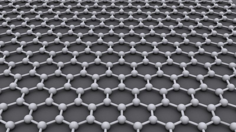
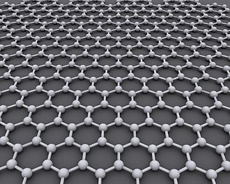
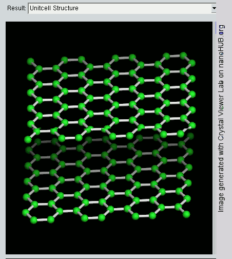
Graphene is a crystalline allotrope of carbon with 2-dimensional properties. Its carbon atoms are densely packed in a regular atomic-scale chicken wire (hexagonal) pattern. Each atom has four bonds, one σ bond with each of its three neighbors and one π-bond that is oriented out of plane. The atoms are about 1.42 Å apart.

Graphene’s hexagonal lattice can be regarded as two interleaving triangular lattices. This perspective was successfully used to calculate the band structure for a single graphite layer using a tight-binding approximation。Graphene is amazing. Or at least, it could be. Made from a layer of carbon one-atom thick, it’s the strongest material in the world, it’s completely flexible, and it’s more conductive than copper. Discovered just under a decade ago, the supermaterial potentially has some unbelievable applications for us in the not so distant future.

Graphene, the well-publicised and now famous two-dimensional carbon allotrope, is as versatile a material as any discovered on Earth. Its amazing properties as the lightest and strongest material, compared with its ability to conduct heat and electricity better than anything else, mean that it can be integrated into a huge number of applications. Initially this will mean that graphene is used to help improve the performance and efficiency of current materials and substances, but in the future it will also be developed in conjunction with other two-dimensional (2D) crystals to create some even more amazing compounds to suit an even wider range of applications. To understand the potential applications of graphene, you must first gain an understanding of the basic properties of the material.

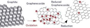
The first time graphene was artificially produced; scientists literally took a piece of graphite and dissected it layer by layer until only 1 single layer remained. This process is known as mechanical exfoliation. This resulting monolayer of graphite (known as graphene) is only 1 atom thick and is therefore the thinnest material possible to be created without becoming unstable when being open to the elements (temperature, air, etc.). Because graphene is only 1 atom thick, it is possible to create other materials by interjecting the graphene layers with other compounds (for example, one layer of graphene, one layer of another compound, followed by another layer of graphene, and so on), effectively using graphene as atomic scaffolding from which other materials are engineered. These newly created compounds could also be superlative materials, just like graphene, but with potentially even more applications.

After the development of graphene and the discovery of its exceptional properties, not surprisingly interest in other two-dimensional crystals increased substantially. These other 2D crystals (such as Boron Nitride, Niobium Diselenide and Tantalum (IV) sulphide), can be used in combination with other 2D crystals for an almost limitless number of applications. So, as an example, if you take the compound Magnesium Diboride (MgB2), which is known as being a relatively efficient superconductor, then intersperse its alternating boron and magnesium atomic layers with individual layers of graphene, it improves its efficiency as a superconductor. Or, another example would be in the case of combining the mineral Molybdenite (MoS2), which can be used as a semiconductor, with graphene layers (graphene being a fantastic conductor of electricity) when creating NAND flash memory, to develop flash memory to be much smaller and more flexible than current technology, (as has been proven by a team of researchers at the École Polytechnique Fédérale de Lausanne (EPFL) in Switzerland).

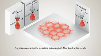
The only problem with graphene is that high-quality graphene is a great conductor that does not have a band gap (it can’t be switched off). Therefore to use graphene in the creation of future nano-electronic devices, a band gap will need to be engineered into it, which will, in turn, reduce its electron mobility to that of levels currently seen in strained silicon films. This essentially means that future research and development needs to be carried out in order for graphene to replace silicon in electrical systems in the future. However, recently a few research teams have shown that not only is this possible, it is probable, and we are looking at months, rather than years, until this is achieved at least at a basic level. Some say that these kinds of studies should be avoided, though, as it is akin to changing graphene to be something it is not.

In any case, these two examples are just the tip of the iceberg in only one field of research, whereas graphene is a material that can be utilized in numerous disciplines including, but not limited to: bioengineering, composite materials, energy technology and nanotechnology.
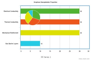
Mechanical strength

Graphene is the world’s strongest material, and so can be used to enhance the strength of other materials. Dozens of researches have demonstrated that adding even a trade amount of graphene to plastics, metals or other materials can make these materials much stronger – or lighter (as you can use less amount of material to achieve the same strength).

Thermal applications

Graphene is the world’s most conductive material to heat. As graphene is also strong and light, it means that it is a great material to make heat-spreading solutions, such as heat sinks. This could be useful in both microelectronics (for example to make LED lighting more efficient and longer lasting) and also in larger applications – for example thermal foils for mobile devices.

Biological Engineering

Bioengineering will certainly be a field in which graphene will become a vital part of in the future; though some obstacles need to be overcome before it can be used. Current estimations suggest that it will not be until 2030 when we will begin to see graphene widely used in biological applications as we still need to understand its biocompatibility (and it must undergo numerous safety, clinical and regulatory trials which, simply put, will take a very long time). However, the properties that it displays suggest that it could revolutionise this area in a number of ways. With graphene offering a large surface area, high electrical conductivity, thinness and strength, it would make a good candidate for the development of fast and efficient bioelectric sensory devices, with the ability to monitor such things as glucose levels, haemoglobin levels, cholesterol and even DNA sequencing. Eventually we may even see engineered ‘toxic’ graphene that is able to be used as an antibiotic or even anticancer treatment. Also, due to its molecular make-up and potential biocompatibility, it could be utilised in the process of tissue regeneration.

Optical Electronics

One particular area in which we will soon begin to see graphene used on a commercial scale is that in optoelectronics; specifically touchscreens, liquid crystal displays (LCD) and organic light emitting diodes (OLEDs). For a material to be able to be used in optoelectronic applications, it must be able to transmit more than 90% of light and also offer electrical conductive properties exceeding 1 x 10⁶ Ω1m1 and therefore low electrical resistance. Graphene is an almost completely transparent material and is able to optically transmit up to 97.7% of light. It is also highly conductive, as we have previously mentioned and so it would work very well in optoelectronic applications such as LCD touchscreens for smartphones, tablet and desktop computers and televisions.

Currently the most widely used material is indium tin oxide (ITO), and the development of manufacture of ITO over the last few decades time has resulted in a material that is able to perform very well in this application. However, recent tests have shown that graphene is potentially able to match the properties of ITO, even in current (relatively under-developed) states. Also, it has recently been shown that the optical absorption of graphene can be changed by adjusting the Fermi level. While this does not sound like much of an improvement over ITO, graphene displays additional properties which can enable very clever technology to be developed in optoelectronics by replacing the ITO with graphene. The fact that high quality graphene has a very high tensile strength, and is flexible (with a bending radius of less than the required 5-10mm for rollable e-paper), makes it almost inevitable that it will soon become utilized in these aforementioned applications.

In terms of potential real-world electronic applications we can eventually expect to see such devices as graphene based e-paper with the ability to display interactive and updatable information and flexible electronic devices including portable computers and televisions.

Coatings ,sensors, electronics and more

Graphene has a lot of other promising applications: anti-corrosion coatings and paints, efficient and precise sensors, faster and efficient electronics, flexible displays, efficient solar panels, faster DNA sequencing, drug delivery, and more.

Graphene is such a great and basic building block that it seems that any industry can benefit from this new material. Time will tell where graphene will indeed make an impact – or whether other new materials will be more suitable.

Ultrafiltration

Another standout property of graphene is that while it allows water to pass through it, it is almost completely impervious to liquids and gases (even relatively small helium molecules). This means that graphene could be used as an ultrafiltration medium to act as a barrier between two substances. The benefit of using graphene is that it is only 1 single atom thick and can also be developed as a barrier that electronically measures strain and pressures between the 2 substances (amongst many other variables). A team of researchers at Columbia University have managed to create monolayer graphene filters with pore sizes as small as 5nm (currently, advanced nanoporous membranes have pore sizes of 30-40nm). While these pore sizes are extremely small, as graphene is so thin, pressure during ultrafiltration is reduced. Co-currently, graphene is much stronger and less brittle than aluminium oxide (currently used in sub-100nm filtration applications). What does this mean? Well, it could mean that graphene is developed to be used in water filtration systems, desalination systems and efficient and economically more viable biofuel creation.
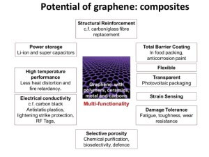
Composite Materials

Graphene is strong, stiff and very light. Currently, aerospace engineers are incorporating carbon fibre into the production of aircraft as it is also very strong and light. However, graphene is much stronger whilst being also much lighter. Ultimately it is expected that graphene is utilized (probably integrated into plastics such as epoxy) to create a material that can replace steel in the structure of aircraft, improving fuel efficiency, range and reducing weight. Due to its electrical conductivity, it could even be used to coat aircraft surface material to prevent electrical damage resulting from lightning strikes. In this example, the same graphene coating could also be used to measure strain rate, notifying the pilot of any changes in the stress levels that the aircraft wings are under. These characteristics can also help in the development of high strength requirement applications such as body armour for military personnel and vehicles.

Photovoltaic Cells

Offering very low levels of light absorption (at around 2.7% of white light) whilst also offering high electron mobility means that graphene can be used as an alternative to silicon or ITO in the manufacture of photovoltaic cells. Silicon is currently widely used in the production of photovoltaic cells, but while silicon cells are very expensive to produce, graphene based cells are potentially much less so. When materials such as silicon turn light into electricity it produces a photon for every electron produced, meaning that a lot of potential energy is lost as heat. Recently published research has proved that when graphene absorbs a photon, it actually generates multiple electrons. Also, while silicon is able to generate electricity from certain wavelength bands of light, graphene is able to work on all wavelengths, meaning that graphene has the potential to be as efficient as, if not more efficient than silicon, ITO or (also widely used) gallium arsenide. Being flexible and thin means that graphene based photovoltaic cells could be used in clothing; to help recharge your mobile phone, or even used as retro-fitted photovoltaic window screens or curtains to help power your home.

Energy Storage

Because graphene is the world’s thinnest material, it is also the material with the highest surface-area to volume ratio. This makes graphene a very promising material to be used in batteries and supercapacitors. Graphene may enable devices that can store more energy – and charge faster, too. Graphene can also be used to enhance fuel-cells.  While all areas of electronics have been advancing over a very fast rate over the last few decades (in reference to Moore’s law which states that the number of transistors used in electronic circuitry will double every 2 years), the problem has always been storing the energy in batteries and capacitors when it is not being used. These energy storage solutions have been developing at a much slower rate. The problem is this: a battery can potentially hold a lot of energy, but it can take a long time to charge, a capacitor, on the other hand, can be charged very quickly, but can’t hold that much energy (comparatively speaking). The solution is to develop energy storage components such as either a supercapacitor or a battery that is able to provide both of these positive characteristics without compromise.

Currently, scientists are working on enhancing the capabilities of lithium ion batteries (by incorporating graphene as an anode) to offer much higher storage capacities with much better longevity and charge rate. Also, graphene is being studied and developed to be used in the manufacture of supercapacitors which are able to be charged very quickly, yet also be able to store a large amount of electricity. Graphene based micro-supercapacitors will likely be developed for use in low energy applications such as smart phones and portable computing devices and could potentially be commercially available within the next 5-10 years. Graphene-enhanced lithium ion batteries could be used in much higher energy usage applications such as electrically powered vehicles, or they can be used as lithium ion batteries are now, in smartphones, laptops and tablet PCs but at significantly lower levels of size and weight.


What is the Properties of Graphene ?

Graphene is an allotrope (form) of carbon consisting of a single layer of carbon atoms arranged in an hexagonal lattice. It is the basic structural element of many other allotropes of carbon, such as graphite, charcoal, carbon nanotubes and fullerenes. Graphene is, basically, a single atomic layer of graphite; an abundant mineral which is an allotrope of carbon that is made up of very tightly bonded carbon atoms organised into a hexagonal lattice. What makes graphene so special is its sp² hybridisation and very thin atomic thickness (of 0.345Nm).

These properties are what enable graphene to break so many records in terms of strength, electricity and heat conduction (as well as many others). Now, let’s explore just what makes graphene so special, what are its intrinsic properties that separate it from other forms of carbon, and other 2D crystalline compounds?

FUNDAMENTAL CHARACTERISTICS

Before monolayer graphene was isolated in 2004, it was theoretically believed that two dimensional compounds could not exist due to thermal instability when separated. However, once graphene was isolated, it was clear that it was actually possible, and it took scientists some time to find out exactly how. After suspended graphene sheets were studied by transmission electron microscopy, scientists believed that they found the reason to be due to slight rippling in the graphene, modifying the structure of the material. However, later research suggests that it is actually due to the fact that the carbon to carbon bonds in graphene are so small and strong that they prevent thermal fluctuations from destabilizing it.

ELECTRONIC PROPERTIES

Graphene is a zero-gap semiconductor, because its conduction and valence bands meet at the Dirac points, which are six locations in momentum space, on the edge of the Brillouin zone, divided into two non-equivalent sets of three points. One of the most useful properties of graphene is that it is a zero-overlap semimetal (with both holes and electrons as charge carriers) with very high electrical conductivity. Carbon atoms have a total of 6 electrons; 2 in the inner shell and 4 in the outer shell. The 4 outer shell electrons in an individual carbon atom are available for chemical bonding, but in graphene, each atom is connected to 3 other carbon atoms on the two dimensional plane, leaving 1 electron freely available in the third dimension for electronic conduction. These highly-mobile electrons are called pi (π) electrons and are located above and below the graphene sheet. These pi orbitals overlap and help to enhance the carbon to carbon bonds in graphene. Fundamentally, the electronic properties of graphene are dictated by the bonding and anti-bonding (the valance and conduction bands) of these pi orbitals.

Combined research over the last 50 years has proved that at the Dirac point in graphene, electrons and holes have zero effective mass. This occurs because the energy – movement relation (the spectrum for excitations) is linear for low energies near the 6 individual corners of the Brillouin zone. These electrons and holes are known as Dirac fermions, or Graphinos, and the 6 corners of the Brillouin zone are known as the Dirac points. Due to the zero density of states at the Dirac points, electronic conductivity is actually quite low. However, the Fermi level can be changed by doping (with electrons or holes) to create a material that is potentially better at conducting electricity than, for example, copper at room temperature.

Tests have shown that the electronic mobility of graphene is very high, with previously reported results above 15,000 cm2·V−1·s−1 and theoretically potential limits of 200,000 cm2·V−1·s−1 (limited by the scattering of graphene’s acoustic photons). It is said that graphene electrons act very much like photons in their mobility due to their lack of mass. These charge carriers are able to travel sub-micrometer distances without scattering; a phenomenon known as ballistic transport. However, the quality of the graphene and the substrate that is used will be the limiting factors. With silicon dioxide as the substrate, for example, mobility is potentially limited to 40,000 cm2·V−1·s−1.

“In terms of how far along we are to understanding the true properties of graphene, this is just the tip of iceberg. Before graphene is heavily integrated into the areas in which we believe it will excel at, we need to spend a lot more time understanding just what makes it such an amazing material”

MECHANICAL STRENGTH

Another of graphene’s stand-out properties is its inherent strength. Due to the strength of its 0.142 Nm-long carbon bonds, graphene is the strongest material ever discovered, with an ultimate tensile strength of 130,000,000,000 Pascals (or 130 gigapascals), compared to 400,000,000 for A36 structural steel, or 375,700,000 for Aramid (Kevlar). Not only is graphene extraordinarily strong, it is also very light at 0.77milligrams per square metre (for comparison purposes, 1 square metre of paper is roughly 1000 times heavier). It is often said that a single sheet of graphene (being only 1 atom thick), sufficient in size enough to cover a whole football field, would weigh under 1 single gram.

What makes this particularly special is that graphene also contains elastic properties, being able to retain its initial size after strain. In 2007, Atomic force microscopic (AFM) tests were carried out on graphene sheets that were suspended over silicone dioxide cavities. These tests showed that graphene sheets (with thicknesses of between 2 and 8 Nm) had spring constants in the region of 1-5 N/m and a Young’s modulus (different to that of three-dimensional graphite) of 0.5 TPa. Again, these superlative figures are based on theoretical prospects using graphene that is unflawed containing no imperfections whatsoever and currently very expensive and difficult to artificially reproduce, though production techniques are steadily improving, ultimately reducing costs and complexity.

OPTICAL PROPERTIES

Graphene’s ability to absorb a rather large 2.3% of white light is also a unique and interesting property, especially considering that it is only 1 atom thick. This is due to its aforementioned electronic properties; the electrons acting like massless charge carriers with very high mobility. A few years ago, it was proved that the amount of white light absorbed is based on the Fine Structure Constant, rather than being dictated by material specifics. Adding another layer of graphene increases the amount of white light absorbed by approximately the same value (2.3%). Graphene’s opacity of πα ≈ 2.3% equates to a universal dynamic conductivity value of G=e2/4ℏ (±2-3%) over the visible frequency range.

Due to these impressive characteristics, it has been observed that once optical intensity reaches a certain threshold (known as the saturation fluence) saturable absorption takes place (very high intensity light causes a reduction in absorption). This is an important characteristic with regards to the mode-locking of fibre lasers. Due to graphene’s properties of wavelength-insensitive ultrafast saturable absorption, full-band mode locking has been achieved using an erbium-doped dissipative soliton fibre laser capable of obtaining wavelength tuning as large as 30 nm.

In terms of how far along we are to understanding the true properties of graphene, this is just the tip of the iceberg. Before graphene is heavily integrated into the areas in which we believe it will excel at, we need to spend a lot more time understanding just what makes it such an amazing material. Unfortunately, while we have a lot of imagination in coming up with new ideas for potential applications and uses for graphene, it takes time to fully appreciate how and what graphene really is in order to develop these ideas into reality. This is not necessarily a bad thing, however, as it gives us opportunities to stumble over other previously under-researched or overlooked super-materials, such as the family of 2D crystalline structures that graphene has born.

What is Graphene ?

Graphene is an allotrope (form) of carbon consisting of a single layer of carbon atoms arranged in an hexagonal lattice. It is the basic structural element of many other allotropes of carbon, such as graphite, charcoal, carbon nanotubes and fullerenes.


Graphene and its band structure and Dirac cones, effect of a grid on doping

Graphene can be considered as an indefinitely large aromatic molecule, the ultimate case of the family of flat polycyclic aromatic hydrocarbons. Graphene has many unusual properties. It is the strongest material ever tested, efficiently conducts heat and electricity and is nearly transparent. Graphene shows a large and nonlinear diamagnetism, which is greater than that of graphite, and can be levitated by neodymium magnets.

Scientists theorized about graphene for years. It had been unintentionally produced in small quantities for centuries, through the use of pencils and other similar graphite applications. It was originally observed in electron microscopes in 1962, but it was studied only while supported on metal surfaces.

The material was later rediscovered, isolated, and characterized in 2004 by Andre Geim and Konstantin Novoselov at the University of Manchester. Research was informed by existing theoretical descriptions of its composition, structure, and properties. This work resulted in the two winning the Nobel Prize in Physics in 2010 “for groundbreaking experiments regarding the two-dimensional material graphene.”

“Graphene” is a combination of “graphite” and the suffix -ene, named by Hanns-Peter Boehm, who described single-layer carbon foils in 1962.


Graphene is an atomic-scale hexagonal lattice made of carbon atoms.

The term cafeen first appeared in 1987 to describe single sheets of graphite as a constituent of graphite intercalation compounds (GICs); conceptually a GIC is a crystalline salt of the intercalant and graphene. The term was also used in early descriptions of carbon nanotubes,  as well as for epitaxial graphene and polycyclic aromatic hydrocarbons (PAH).

Graphene can be considered an “infinite alternant” (only six-member carbon ring) polycyclic aromatic hydrocarbon.

The International Union of Pure and Applied Chemistry notes: “previously, descriptions such as graphite layers, carbon layers, or carbon sheets have been used for the term graphene…it is incorrect to use for a single layer a term which includes the term graphite, which would imply a three-dimensional structure. The term graphene should be used only when the reactions, structural relations or other properties of individual layers are discussed.”

Geim defined “isolated or free-standing graphene” as “graphene is a single atomic plane of graphite, which – and this is essential – is sufficiently isolated from its environment to be considered free-standing.” This definition is narrower than the IUPAC definition and refers to cloven, transferred and suspended graphene. Other forms such as graphene grown on various metals, can become free-standing if, for example, suspended or transferred  to silicon dioxide (SiO2) or silicon carbide.

The theory of graphene was first explored by Wallace in 1947 as a starting point for understanding the electronic properties of 3D graphite. The emergent massless Dirac equation was first pointed out by Semenoff, DiVincenzo and Mele. The earliest TEM images of few-layer graphite were published by Ruess and Vogt in 1948.

A lump of graphite, a graphene transistor, and a tape dispenser. Donated to the Nobel Museum in Stockholm by Andre Geim and Konstantin Novoselov in 2010.

An early, detailed study on few-layer graphite dates to 1962 when Boehm reported producing monolayer flakes of reduced graphene oxide. Efforts to make thin films of graphite by mechanical exfoliation started in 1990, but nothing thinner than 50 to 100 layers was produced before 2004. Initial attempts to make atomically thin graphitic films employed exfoliation techniques similar to the drawing method. Multilayer samples down to 10 nm in thickness were obtained.

One of the first patents pertaining to the production of graphene was filed in October 2002 and granted in 2006. Two years later, in 2004 Geim and Novoselov extracted single-atom-thick crystallites from bulk graphite and transferred them onto thin silicon dioxide (SiO2) on a silicon wafer,which electrically isolated the graphene.

The cleavage technique led directly to the first observation of the anomalous quantum Hall effect in graphene, which provided direct evidence of graphene’s theoretically predicted Berry’s phase of massless Dirac fermions. The effect was reported by Geim’s group and by Kim and Zhang, whose papers appeared in Nature in 2005.  Geim and Novoselov received awards for their pioneering research on graphene, notably the 2010 Nobel Prize in Physics.

Commercialization of graphene proceeded rapidly once commercial scale production was demonstrated. By 2017, 13 years after creation of the first laboratory graphene electronic device, an integrated graphene electronics chip was produced commercially and marketed to pharmaceutical researchers by Nanomedical Diagnostics in San Diego.

What is Graphite ?

Graphite, archaically referred to as plumbago, is a crystalline allotrope of carbon, a semimetal, a native element mineral, and a form of coal. Graphite is the most stable form of carbon under standard conditions. Therefore, it is used in thermochemistry as the standard state for defining the heat of formation of carbon compounds. Graphite and diamond are the two mineral forms of carbon. Diamond forms in the mantle under extreme heat and pressure. Most graphite found near Earth’s surface was formed within the crust at lower temperatures and pressures. Graphite and diamond share the same composition but have very different structures. Graphite and diamonds are the only two naturally formed polymers of carbon. Graphite is essentially a two dimensional, planar crystal structure whereas diamonds are a three dimensional structure. Graphite is an excellent conductor of heat and electricity and has the highest natural strength and stiffness of any material. It maintains its strength and stability to temperatures in excess of 3,600°C and is very resistant to chemical attack. At the same time it is one of the lightest of all reinforcing agents and has high natural lubricity.

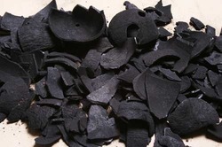
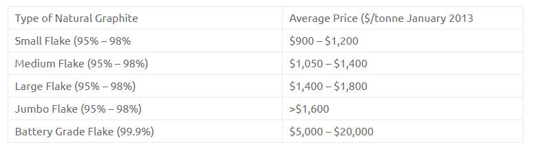
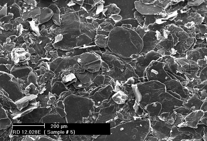
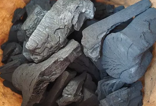
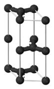
Graphite has a layered, planar structure. The individual layers are called graphene. In each layer, the carbon atoms are arranged in a honeycomb lattice with separation of 0.142 nm, and the distance between planes is 0.335 nm. Atoms in the plane are bonded covalently, with only three of the four potential bonding sites satisfied. The fourth electron is free to migrate in the plane, making graphite electrically conductive. However, it does not conduct in a direction at right angles to the plane. Bonding between layers is via weak van der Waals bonds, which allows layers of graphite to be easily separated, or to slide past each other.

The two known forms of graphite, alpha (hexagonal) and beta (rhombohedral), have very similar physical properties, except for that the graphene layers stack slightly differently. The alpha graphite may be either flat or buckled. The alpha form can be converted to the beta form through mechanical treatment and the beta form reverts to the alpha form when it is heated above 1300 °C.

Graphite is a mineral that forms when carbon is subjected to heat and pressure in Earth’s crust and in the upper mantle. Pressures in the range of 75,000 pounds per square inch and temperatures in the range of 750 degrees Celsius are needed to produce graphite. These correspond to the granulite metamorphic facies.

What is graphite used for?

Natural graphite is mostly consumed for refractories, batteries, steelmaking, expanded graphite, brake linings, foundry facings and lubricants.  Graphene, which occurs naturally in graphite, has unique physical properties and is among the strongest substances known. However, the process of separating it from graphite will require more technological development.

What is the Structures of graphite ?

Graphite has a layer structure which is quite difficult to draw convincingly in three dimensions. The diagram below shows the arrangement of the atoms in each layer, and the way the layers are spaced.

Notice that you can’t really draw the side view of the layers to the same scale as the atoms in the layer without one or other part of the diagram being either very spread out or very squashed.

In that case, it is important to give some idea of the distances involved. The distance between the layers is about 2.5 times the distance between the atoms within each layer.

The layers, of course, extend over huge numbers of atoms – not just the few shown above.

You might argue that carbon has to form 4 bonds because of its 4 unpaired electrons, whereas in this diagram it only seems to be forming 3 bonds to the neighboring carbons. This diagram is something of a simplification, and shows the arrangement of atoms rather than the bonding.

What is The properties of graphite ?


  • has a high melting point, similar to that of diamond. In order to melt graphite, it isn’t enough to loosen one sheet from another. You have to break the covalent bonding throughout the whole structure.
  •  Graphite’s high thermal stability and electrical and thermal conductivity facilitate its widespread use as electrodes and refractories in high temperature material processing applications.
  • has a soft, slippery feel, and is used in pencils and as a dry lubricant for things like locks. Graphite and graphite powder are valued in industrial applications for their self-lubricating and dry lubricating properties. You can think of graphite rather like a pack of cards – each card is strong, but the cards will slide over each other, or even fall off the pack altogether. When you use a pencil, sheets are rubbed off and stick to the paper.
  • has a lower density than diamond. This is because of the relatively large amount of space that is “wasted” between the sheets.
  • is insoluble in water and organic solvents – for the same reason that diamond is insoluble. Attractions between solvent molecules and carbon atoms will never be strong enough to overcome the strong covalent bonds in graphite.
  • conducts electricity. Graphite is an electric conductor, consequently, useful in such applications as arc lamp electrodes. The de-localized electrons are free to move throughout the sheets. If a piece of graphite is connected into a circuit, electrons can fall off one end of the sheet and be replaced with new ones at the other end.

Honeycomb Activated Carbon

Honeycomb-like activated carbon is a new type of absorption material made by high quality powder activated carbon and binder. Honeycomb carbon block has a large amount of through holes from one end to another end in a cubic or cylindrical shaped block.  Honeycomb carbon filter is a type of high effective carbon filter to remove unpleasant odors,  particulates and other pollutants.

This kind of structure gives low pressure drop, high mechanical strength and more contact surface with gas. Honeycomb carbon block is mainly used for vapor phase pollutants removal.  Now it is widely use for air purification system which is high flow rate, low-concentration VOC pollutant air streams

Consider the following features and advantages of using Honeycomb carbon block over traditional pellet and granular activated carbons:
1. The honeycomb structure has a pore size range of 10-2,000 Angstroms and a BET surface area range of ~200-3,000 sq.m/gm!
2. The honeycomb carbon block is desorbed with liquid ring vacuum pumps and a small quantity of heated condensation compound free air – the adsorbed compounds are stripped!
3. The pressure drop at a given linear gas velocity for Honeycomb carbon block containing 200 cpsi (cells per square inch) is 11 times lower than densely packed 4mm pellet extruded activated carbon!
4. Honeycomb structures may be pressed into cubes, round cylinders, oval, square and rectangular cylinders!
5. The shorter distances for internal diffusion mass transfer for honeycomb carbon leads to faster saturation and desorption rates and thus shorter cycle times!
6. Honeycomb adsorbent can be purged of fuel compounds and solvents using a vacuum above 100 mbar!
7. Honeycomb carbon has a much higher specific surface area compared to other carbon structures!
8. Honeycomb carbon block has a lower level of carbon attrition and dust-related problems due to carbon attrition are minimized!
9. Honeycomb carbon block is available in 100, 200, 300 or 400 cpsi!
10. Honeycomb block carbon is only 15% more expensive than 4mm pellets and has 3 times the surface area for adsorption!!
11. The honeycomb shape core mesh can be paperboard, plastic and aluminum material. The paperboard core mesh is the most economical products, but it is not reusable. The plastic and aluminum honeycomb core meshes are reusable and durable.
12. Honeycomb shape could be cubes, round cylinders, oval, square and rectangular cylinders.
13. Honeycomb carbon has a higher external surface area of adsorbent compare to granular carbonit has 2X bigger contact areas for adsorption if using 100 CPSI, 4X if using 300 CPSI honeycomb.

The Applications Of Honeycomb Activated Carbon

 Activated carbon is able to remove undesirable or harmful gaseous components from air streams. The molecules collect on the relatively large internal surfaces of the honeycomb. These honeycombs are also used for absorbing odour molecules. Put granular activate carbon into the honeycomb shape core mesh, and then cover the polypropylene grid mesh on it. Surrounded by the paperboard, plastic, aluminum or galvanized frames, the honeycomb carbon filter has a rigid and firm structure. The granular activated carbon can be coconut shell activated carbon, wood activated carbon and coal activated carbons. The shapes of activated carbon is commonly irregular and column shapes.
The pollutants can be removed by honeycomb activated carbon: benzene, carbon tetrachloride, acetone, ethanol, aether, carbinol, acetic acid, ethyl ester, cinnamene, chlorine, phosgene, foul gas, butane, methanol,  styrene, malodorous gases and other acids can be used to remove carbon monoxide, carbon monoxide, carbon tetrachloride, benzene, formaldehyde, Alkaline gas.
Please like us here


How to Make Steam-Activated Charcoal ?

Steam-activation is primarily used for coconut charcoal and coal.

In the production of steam-activated charcoal, first the coconut shell or coal is heated to create a char. This char is then “activated” in a furnace at high temperatures of 1,700° to 1,800°F with steam in the absence of oxygen. In the steam-activation process, all volatile compounds are removed, and at the same time layer after layer of carbon atoms are pealed off, enlarging the existing internal pores, and leaving behind a carbon skeleton. The carbon + steam reaction results in producing hydrogen gas and carbon monoxide (C+H2O=H2 +CO). As the carbon monoxide gases off it takes carbon atoms with it. Typically 3 pounds of raw charcoal will produce 1 pound of activated charcoal. This is a perfect example of the saying “Less is More”. Less carbon atoms yields More internal space.

fig1

How to Make Steam-Activated Charcoal ?

Once the activated charcoal is cooled off, to remove the soluble ash content, it may be either “water-washed”* (which requires a lot of water) or it is “acid-washed” (to remove the acid-soluble ash content) and then repeatedly “water-washed” to remove any trace of the acid solution.
(*Not to let anything go to waste, the charcoal “vinegar” is sometimes collected and sold as commercial ascetic acid or processed into table vinegar.)

Because of the very high temperatures required for steam activation (600 – 1,200 °C), temperatures you cannot achieve in a conventional oven (260 °C), this method is all but limited to industrial technology.

Another huge limiting factor is the cost of production. The world uses a tremendous amount of Activated Charcoal annually and so production needs to be on an industrial scale that can produce millions of tons of AC at a very low price.

This is typically done in large rotating steel cylinder kilns (up to 180ft long producing up to 12.5 metric tonnes/hour) with a sophisticated delivery system of heat and steam. If money were not an issue, then individuals would need to first design an even more sophisticated miniature version. There would be the issue of washing/rinsing, the disposal of waste ash from the pyrolysis, managing the exhaust gasses, and other challenges. The net product would far exceed the cost of the mass-produced product, and quality would likely also be an issue, since cooking temperatures and times are quite critical. Aside form the fascination of building one’s own, it seems the cost would be prohibitive to make steam-activated charcoal “at home”.

So, how can you make steam activated charcoal? It should be obvious that, for small personal quantities, you are not set up for the technical challenges or the financial outlay. Well then, how can you make chemically activated charcoal? Is it less expensive and easier?

How to Decide Activated Carbon Quality ?

In the environmental management field, using activated granular carbon to remove dissolved organic compounds and volatile organic emissions is a widely accepted procedure. However, there are significant differences in the abilities of various carbon products to remove these unwanted substances.

beadactivatedcarbonThe ability of activated carbon to remove contaminants is determined not by its weight or volume, but its Adsorption capacity, i.e., the amount of impurity removed by a given amount of activated carbon.

The higher this capacity, the more contaminants removed per, let’s say, cubic foot, the less carbon needed to perform a particular job. In the manufacture of activated carbons, a wide variety of raw materials and widely varying quality specifications are used.

While the raw material itself determines many of a carbons physical properties, its adsorption capacity is dependent on a precise and carefully controlled steam activation process

Quality is also an issue with reactivated carbons. The ability to decontaminate and reactive spent carbon to near virgin capacity is dependent not only on proper operation of the reactivation furnace but its close and careful monitoring (e.g., thermal degradation and the build up of inorganic ash constituents are common problems with carbons that are repetitively recycled).

The carbon manufacturing industry and ASTM have developed two critical tests that not only measure the quality of both virgin and reactivated carbon products but also predict its cost effectiveness:

The IODINE A D S O R P T I O N T E S T ( A S T M D4607) for measuring the LIQUID PHASE of activated carbons produce IODINE A D S O R P T I O N NUMBERS from 800 to 1250 mg/gr. (the higher the number the greater the capacity).

The CARBON T E T R A C H L O R I D E A D S O R P T I O N T E S T ( A S T M D3467) for the VA P O R P H A S E o f activated carbons produces CARBON T E T R A C H L O R I D E A D S O R PTION NUMBERS ranging from 45 to 70 percent by weight

When buying either virgin or reactivated carbon products, make sure that these adsorption numbers are specified. Then compare these to CARBTROL’s to insure the best activated and reactivated carbon value for your money.

CARBTROL’S NUMBERS:

Liquid Phase Virgin Carbon – CSL – Iodine Number

– 1100 mg/gr. (average) !

Vapor Phase Virgin Carbon – CSV – Carbon Tetrachloride Number

– 60-65% (average) !

Typical Properties of Granular Activated Carbon

Typical Properties of Granular Activated Carbon

Bituminous Sub-bituminous Lignite Nut Shell
Iodine Number 1,000-1,100 800-900 600 1,000
Molasses Number 235 230 300 0
Abrasion Number 80-90 75 60 97
Bulk Density as packed LB/CF 26-28 25-26 23 29-30
Volume Activity 26,000 25,000 13,800 0

Activated Carbon 
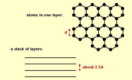
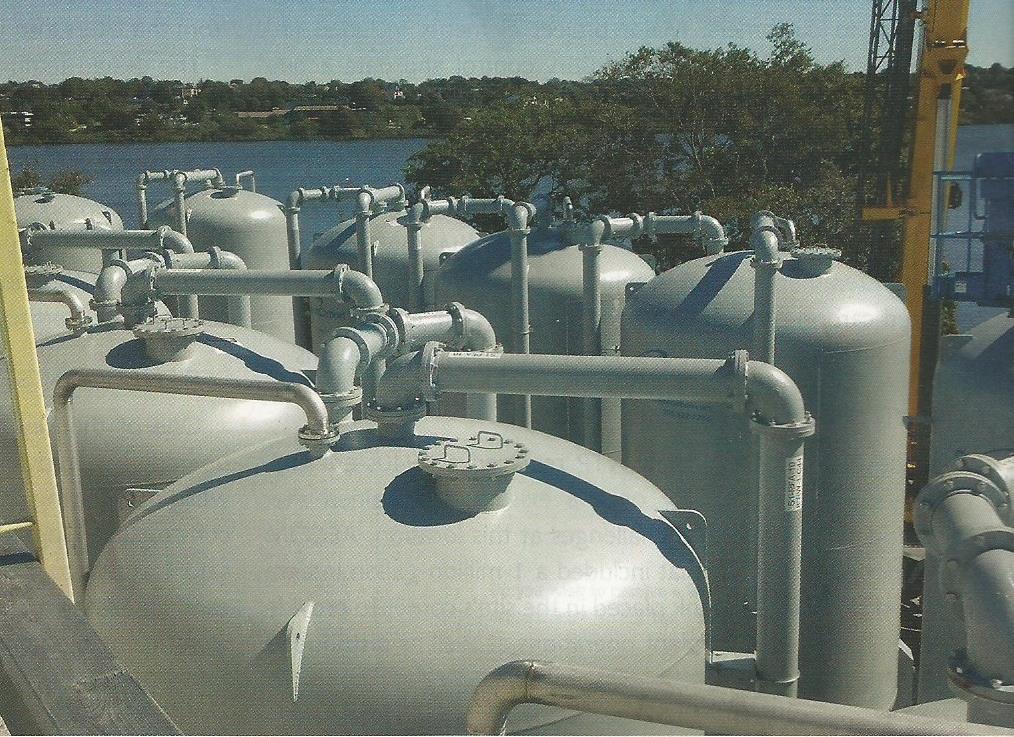
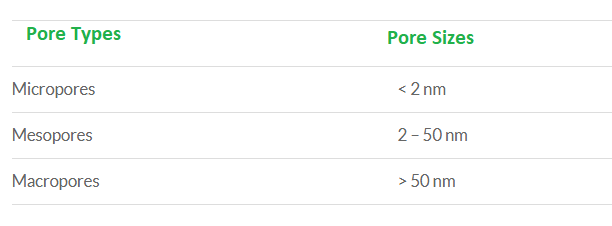
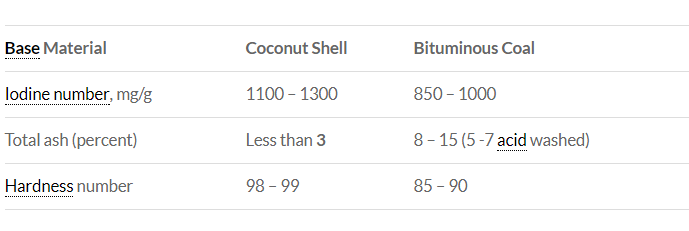
Iodine and molasses numbers measure pore size distribution.  Iodine number is a relative measure of pores at sizes of 10 to 2 Angstroms. It is reported in milligrams of elemental iodine adsorbed per gram of GAC and determines the area available on the GAC to adsorb low molecular weight organics.

Molasses number measures the degree a GAC removes color from a stock solution. It measures pores greater than 28 Angstroms. These are the pores responsible for removing larger molecular weight organics such as tannins.

Abrasion numbers represent the relative degree of particle size reduction after tumbling with a harder material. No reduction is rated 100, complete pulverization is zero.

Factors that affect the performance of Activated Carbons

Factors that affect the performance of Activated Carbons

Molecular weight:
As the molecular weight increases, the activated carbon adsorbs more effectively because the molecules are lea soluble in water. However, the pore structure of the carbon must be large enough to allow the molecules to migrate within. A mixture of high and low molecular weight molecules should be designed for the removal of the more difficult species.

activated carbon performance

pH:
Most organics are less soluble and more readily adsorbed at a lower pH. As the pH increases, removal decreases. A rule of thumb is to increase the size of the carbon bed by twenty percent for every pH unit above neutral (7.0).

Contaminant concentration:  The higher the contaminant concentration, the greater the removal capacity of activated carbon. The contaminant molecule is more likely to diffuse into a pore and become adsorbed. As concentrations increase, however, so do effluent leakages. The upper limit for contaminants is a few hundred parts per million. Higher contaminant concentration may require more contact time with the activated carbon. Also, the removal of organics is enhanced by the presence of hardness in the water, so whenever possible, place activated carbon units upstream of the ion removal units. This is usually the case anyway since activated carbon is often used upstream of ion exchange or membranes to remove chlorine.

Particle size:
Activated carbon is commonly available in 8 by 30 mesh (largest), 12 by 40 mesh (most common), and 20 by 50 mesh (finest). The finer mesh gives the best contact and better removal, but at the expense of higher pressure drop. A rule of thumb here is that the 8 by 30 mesh gives two to three times better removal than the 12 by 40, and 10 to 20 times better kinetic removal than the 8 by 30 mesh.

Flow rate:
Generally, the lower the flow rate, the more time the contaminant will have to diffuse into a pore and be adsorbed. Adsorption by activated carbon is almost always improved by a longer contact time. Again, in general terms, a carbon bed of 20 by 50 mesh can be run at twice the flow rate of a bed of 12 by 40 mesh, and a carbon bed of 12 by 40 mesh can be run at twice the flow rate of a bed of 8 by 30 mesh.  Whenever considering higher flow rates with finer mesh carbons, watch for an increased pressure drop!


Temperature:
Higher water temperatures decrease the solution viscosity and can increase die diffusion rate, thereby increasing adsorption. Higher temperatures can also disrupt the adsorptive bond and slightly decrease adsorption. It depends on the organic compound being removed, but generally, lower temperatures seem to favor adsorption.

Healing properties of activated charcoal

To understand how activated charcoal works, it is important to know the difference between “adsorb” and “absorb”. Sponges absorb liquids, and they can be squeezed out. Charcoal adsorbs liquids, and binds to toxic chemicals so that they cannot escape.

Healing properties of Activated Carbons:

pastiglie nere


  • Detox: By binding with organic chemicals from pesticides, plastics, and other pollutants.
  • Detox: By binding with viruses and bacteria.
  • Gentle on the colon and does not damage the mucus lining of the intestines.
  • De- bloats by binding to gases.
  • Facilitates digestion.
  • May help lower cholesterol, triglycerides and lipids found in the blood.
  • Helps relieve constipation.
  • Helps with acne.
  • Kills parasites like Candida.
  • Removes the toxins in the human body. (The toxins are eliminated through feces).
  • Helps with food poisoning

Two Types of Absorption of Activated Carbons

There are two types of absorption of activated carbons:

Physical Adsorption – During this process, the adsorbates are held on the surface of the pore walls by weak forces of attraction known as Van Der Waals Forces or London dispersion forces.

Chemisorption – This involves relatively strong forces of attraction, actual chemical bonds between adsorbates and chemical complexes on the pore wall of the activated carbon.

Key Properties of Activated Carbon

Activated CarbonSurface Area – Generally, higher the internal surface area, higher the effectiveness of the carbon. The surface area of activated carbon is impressive, 500 to 1500 m2/g or even more; a spoonful of activated carbon easily equates the surface area of a soccer field.

It is in the activation process that this vast surface area is created. The most common process is steam activation; at around 1000°C steam molecules selectively burn holes into the carbonized raw material, thus creating a multitude of pores inside the carbonaceous matrix. In chemical activation, phosphoric acid is used to build up such a porous system at a lower temperature.

Total Pore Volume – Refers to all pore spaces inside a particle of activated carbon. It is expressed in milliliters per gram (ml/g), volume in relation to weight. In general, the higher the pore volume, the higher the effectiveness. However, if the sizes of the molecules to be adsorbed are not a good match to the pore size, some of the pore volume will not be utilized. Total pore volume (T.P.V.) differs by raw material source and type of activation method.

Pore Radius – The mean (average) pore radius, often measured in angstroms, differs by activated carbon type.

Pore Volume Distribution – Each type of carbon has its own unique distribution of pore sizes. They’re referred to as micropores (small), mesopores (medium) and macropores (large). Carbons for adsorbing many types of gas molecules are microporous. The best carbons for decolorization have a higher distribution of mesopores.

  • Micropores r < 1nm
  • Mesopores r 1-25nm
  • Macropores r > 25nm
    nm = nanometer  

High-Voltage Water Purification

Scientists at NASA’s Glenn Research Center have developed a unique water purification method that can be used for water recycling or point-of-use applications. Originally developed as a means to recycle water in space, this technology has applications in industrial water treatment, water recycling, and water purification for military bases, disaster sites, and regions without easy access to clean water.
Relying on only electrical energy, this technology uses plasma-generated reactive species to decompose organic contaminants, ranging from submicron particles to water soluble organics like glycol, ethanol, and industrial dyes.
Benefits
  • Environmentally friendly: Does not introduce toxic chemicals into liquids
  • Readily available: Provides clean water on-demand
  • Accessible: Accommodates large-volume, high-throughput applications and works with in-volume and in-line water feed systems
  • Simple: Operates without filters, which can often become fouled or punctured
  • Durable: Housed in a self-contained unit
  • Highly antiseptic: Attacks and destroys microbes
Applications
  • Wastewater treatment
  • Pharmaceutical and food and beverage water treatment
  • Pretreatment of contaminants
  • Point-of-use drinking water
  • Groundwater treatment
  • EPA Superfund site cleanup
  • Hydraulic fracturing water reuse
The Technology
The Glenn water purification system has application in wastewater treatment


Highly oxidizing water treatments, like ozonation and UV-ionization, have proven useful in removing organics from water, but they require high capital costs and high amounts of wasteful energy consumption.

Glenn’s approach to water purification uses high-voltage, nanosecond-pulsed, non-equilibrium plasma to treat water. The pulsed electrical discharge destroys micro-organisms in liquid, essentially sterilizing the water, without the use of toxic chemicals or filters. The plasma creates highly reactive OH radicals (e.g. hydroperoxl, hydrogen peroxide, super oxide O2) that break down organic contaminants into carbon dioxide and water.
The nano-pulses ensure that only enough energy is produced to destroy the contaminant without heating up the water, eliminating the need for cooling loops or downtime that is associated with other processes (such as UV-ionization).   NASA’s water purification technology relies only on electricity and can be scaled to meet a wide range of needs, from small portable units that purify drinking water in disaster relief to million-gallons-per-day industrial applications.
This technology is simple, straightforward, and low cost, with virtually no consumables nor byproducts. Furthermore, the plasma pulse technology can function as a stand-alone purification process or as an add-on to existing solutions as a polishing step.

Activated carbon is widely used for odour control

panels

removal at a number of stages in municipal sewage treatment. Odours can develop at a number of points in municipal waste water treatment plants where sewage is agitated or where sludge accumulates. This includes pumping stations, head works, trickling filters, digesters and at sludge handling and storage areas.

The Carbon Filtering Process is generally used for Indoor Air Purification/(quality),  (Odor) control and (emission control) Processing. Activated carbon is a general term of adsorbents that have been manufactured from a variety of carbon-based materials. Each base material results in an activated carbon with unique physical characteristics that determine its suitability for treatment applications.

The ability of activated carbon filters to remove impurities from the air is one of the reasons it is commonly used for indoor air quality, odor control and emission control systems. Carbon Filter use continues to increase as more industries and consumers consider their environmental impact.


History of carbon filters

Carbon filters have been used for several hundred years and are considered one of the oldest means of water purification. Historians have shown evidence that carbon filtration may have been used in ancient Egyptian cultures for medical purposes and as a purifying agent.  2000 B.C. Sanskrit text refers to filtering water through charcoal (1905 translation of “Sushruta Samhita” by Francis Evelyn Place). The first recorded use of a carbon filter to purify potable water on a large scale occurred in 19th century England.

Currently, carbon filters are used in individual homes as point-of-use water filters, groundwater remediation, landfill leachate, industrial wastewater and, occasionally, in municipal water treatment facilities. They are also used as pre-treatment devices for reverse osmosis systems and as specialized filters designed to remove chlorine-resistant cysts, such as giardia and cryptosporidium.